


Clock configuration is scary: if it doesn’t work, nothing does, and debugging is not easy. Also, it is very architecture dependent, so there is no one clock tree to rule them all.
STM32 has a nice clock configuration IDE, making it very easy to select the right clock options, so I chose it as an example to show some Zephyr clock tree implementation.
Overview
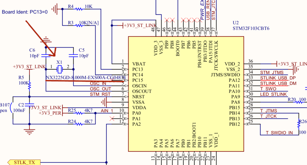
In the Nucleo-F756ZG, the external clock is 8 MHz. Check out the schematics for this NDK NX3225GD-8.0000M crystal ref:
This clock input is also named HSE: High-Speed External oscillator.
If no external clock was present, we could use HSI (High-Speed Internal oscillator), generated in the chip itself, it is less accurate but it saves you an external component.
We also need a Low-Speed clock for low-power stuff, and since there is no 32.768 KHz external clock onboard (aka LSE), we have to use the internal one (aka LSI).
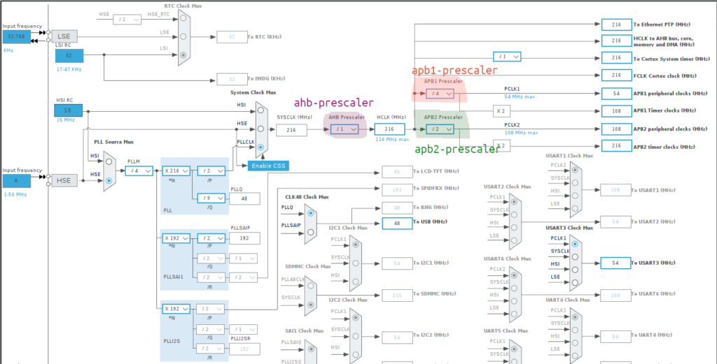
Let’s open STM32CubeIDE Clock Configuration GUI tool:
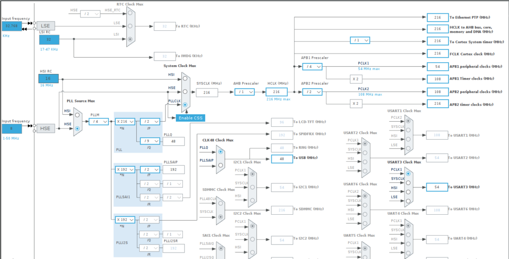
This interface shows the whole clock tree system for the SoC. On the left-hand side, we can see the HSE and LSE external inputs, and how they are muxed with HSI and LSI.
Clock input
Here is the Zephyr device tree description for a high-speed 8MHz external crystal:
clk_hse: clk-hse {
        #clock-cells = <0x0>;
        compatible = "st,stm32-hse-clock";
        status = "okay";
        hse-bypass;
        clock-frequency = <DT_FREQ_M(8)>;
};
./boards/st/nucleo_f756zg/nucleo_f756zg.dts
ⓘ hse-bypass means you are bypassing HSI with HSE, not that you are bypassing HSE. Device tree bindings description states:
hse-bypass: HSE crystal oscillator bypass
Set to the property to by-pass the oscillator with an external clock.
PLL configuration
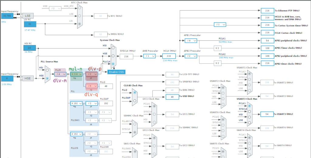
The PLL (Phased-Locked Loop) is a hardware thingy allowing to convert one frequency to another. There is a pipeline of fixed-values multiply and divide operations, so you have to play around with maths to get to the values you want. Here we end up with 216MHz derived from the 8MHz input.
pll: pll {
       #clock-cells = <0x0>;
       compatible = "st,stm32f7-pll-clock";
       status = "okay";
       div-m = <4>;
       mul-n = <216>;
       div-p = <2>;
       div-q = <9>;
       clocks = <&clk_hse>;
};
Compiled ./build/zephyr/zephyr.dts
If the CubeIDE way is not your way, it is possible to use pen and paper and calculator.
- 8 / 4 * 216 / 2 = 216 MHz
- 8 / 4 * 216 / 9 = 48 MHz
RCC block
RCC means “Reset and Clock Control”, it is the hardware peripheral block between your clock input and the different blocks you need to feed clocks to.
&rcc {
        clocks = <&pll>;
        clock-frequency = <DT_FREQ_M(216)>;
        ahb-prescaler = <1>;
        apb1-prescaler = <4>;
        apb2-prescaler = <2>;
};
Compiled ./build/zephyr/zephyr.dts
Peripheral clocks
Peripherals are fed by APB1 and APB2 clocks.
For instance, GPIOA and GPIOB are on APB1 bus. Usually this clock configuration is hidden away in dts include provided by your manufacturer, so you can just call “gpioa” and add your user-related settings.
RCC AHB1 peripheral clock register (RCC_AHB1ENR)
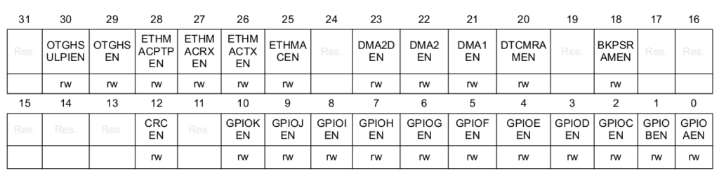
Extract from STM32F75xxx reference manual
gpioa: gpio@40020000 {
        [...]
        clocks = <&rcc STM32_CLOCK_BUS_AHB1 0x00000001>;
};
gpiob: gpio@40020000 {
        [...]
        clocks = <&rcc STM32_CLOCK_BUS_AHB1 0x00000002>;
};
./dts/arm/st/f7/stm32f7.dtsi
Timers, counters and PWM
Timers are plugged to an RCC clock like any other peripherals.
They can have PWM or counter children nodes.
An example with the PWM blinky sample with nucleo_f091rc:
timers2: timers@40000000 {
        compatible = "st,stm32-timers";
        reg = < 0x40000000 0x400 >;
        clocks = < &rcc 0x1c 0x1 >;
        resets = < &rctl 0x200 >;
        interrupts = < 0xf 0x0 >;
        interrupt-names = "global";
        st,prescaler = < 0x2710 >;
        status = "okay";
        pwm2: pwm {
                compatible = "st,stm32-pwm";
                status = "okay";
                #pwm-cells = < 0x3 >;
                pinctrl-0 = < &tim2_ch1_pa5 >;
                pinctrl-names = "default";
                phandle = < 0x21 >;
        };
        counter {
                compatible = "st,stm32-counter";
                status = "disabled";
        };
};
pwmleds: pwmleds {
compatible = "pwm-leds";
status = "okay";
green_pwm_led: green_pwm_led {
pwms = < &pwm2 0x1 0x1312d00 0x0 >;
};
};Conclusion
I hope I managed to convince you, and myself, that clocks configuration is not so scary after all. And if you want the secret method used by the best engineers I know, it is to print the clock tree diagram and use pens and highlighters to mark clock paths choices and selected values.
And make it beautiful.